

AMD patents a chiplet GPU design quite unlike Nvidia and Intel's
Something to look forrad to: AMD has published its beginning patent on chiplet GPU designs. In typical AMD fashion, they're trying to not rock the boat. Chiplet GPUs are simply beginning to emerge. Intel has been forthright well-nigh their development process and confirmed the employment of chiplets in their showtime-generation discrete GPUs. Nvidia, while coy about specifics, accept published numerous inquiry papers on the topic. AMD was the last holdout – which only adds to the intrigue.
Chiplets, equally the name suggests, are smaller less complex chips, that meant to work together into more powerful processors. They're arguably the inevitable future for all high-performance components, and, in some cases, the successful nowadays; AMD's apply of chiplet CPU designs has been brilliant.
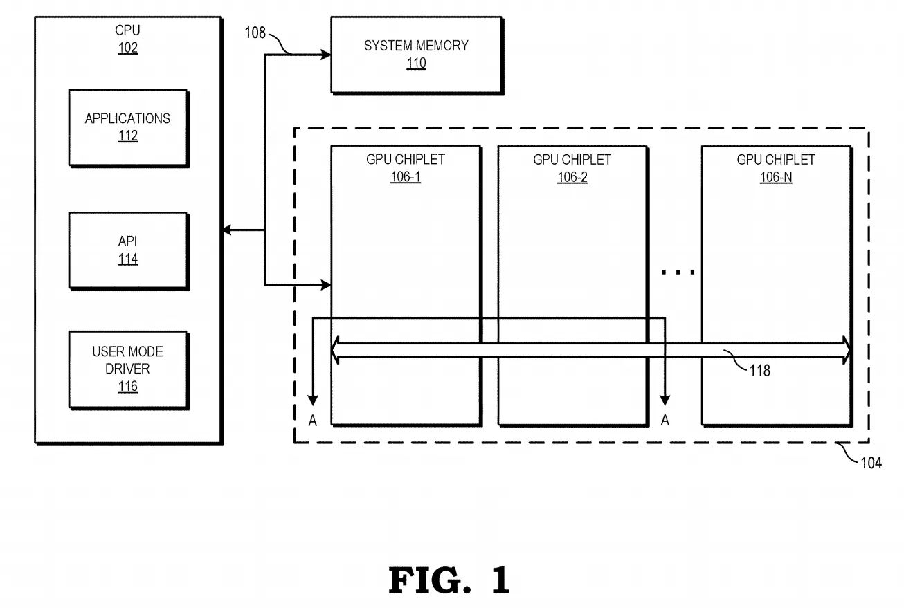
In the new patent dated Dec 31, AMD outlines a chiplet pattern fashioned to mimic a monolithic blueprint as closely every bit possible. Their hypothetical model uses two chiplets connected by a high-speed inactive interposer called a crosslink.
A crosslink connexion sits between the L2 cache and L3 enshroud on the memory bureaucracy. Everything below it, such equally the cores and L1 cache and L2 cache, are aware of their separation from the other chiplet. Everything above, including the L3 cache and GDDR retentiveness, are shared between the chiplets.
This design is benign considering it is conventional. AMD claims that compute units tin can access low-level cache on other chiplets nearly as fast every bit they can admission local depression-level cache. Should that prove true, software won't need updating.
The aforementioned cannot exist said of Intel and Nvidia's designs. Intel intends on using two new technologies, EMIB (embedded multi-die interconnect bridge) and Foveros. The latter is an active interposer that uses through-silicon-vias, something AMD explicitly states they will not employ. Intel's design lets the GPU house a system-attainable cache that powers a new memory fabric.
Nvidia has not disclosed everything, but have indicated a few directions they might pursue. A research paper from 2022 describes a four-chiplet design and a NUMA (non-uniform retentivity access) aware and locality aware compages. Information technology also experiments with a new L1.v cache, which exclusively holds remote data accesses and is bypassed during local retention accesses.
AMD'due south approach might sound the least imaginative, merely it too sounds practical. And if history has proven annihilation, it's that developer-friendliness is a huge advantage.
Below are additional diagrams from the patent.
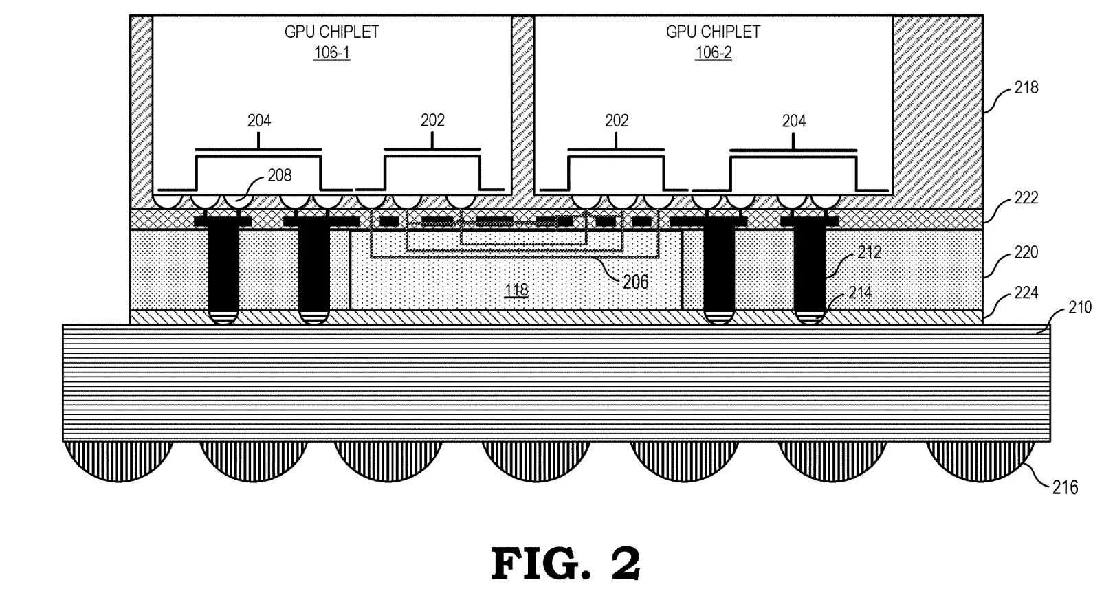
Effigy 2 is a cross-sectional view that descends from ii chiplets to the circuit board. The two chiplets (106-1 and 106-ii) are stacked vertically on the passive crosslink (118) and use dedicated conductor structures to access the crosslink's traces (206) and afterwards communicate with each other. Usher structures not attached to the crosslink (204) connect to the excursion lath for power and other signaling.
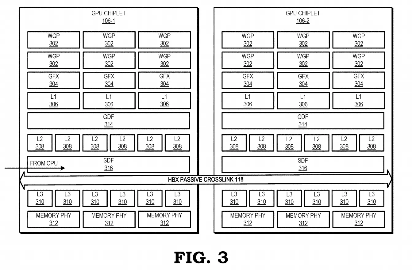
Figure 3 depicts the enshroud hierarchy. WGPs (piece of work grouping processors) (302), which are collections of shader cores, and GFXs (fixed part units) (304), which are defended processors for atypical purposes, connect directly to a aqueduct's L1 enshroud (306). Each chiplet contains multiple L2 enshroud (308) banks that are individually addressable, and also coherent inside a single chiplet. Each chiplet besides contains multiple L3 cache (310) cache banks that are coherent beyond the whole GPU.
The GDF (graphics information fabric) (314) connects the L1 cache banks to the L2 enshroud banks. The SDF (scalable data fabric) (316) combines the L2 cache banks and connects them to the crosslink (118). The crosslink connects to the SDFs on all the chiplets, as well every bit the L3 cache banks on all the chiplets. The GDDR memory lanes (written equally Retention PHY) (312) connect to L3 cache banks.
Equally an case, if a WGP on i chiplet required data from a GDDR banking concern on some other chiplet, that data would be sent through to an L3 cache bank, and then over the crosslink to an SDF, then to an L2 bank, and finally, through a GDF to an L1 bank.
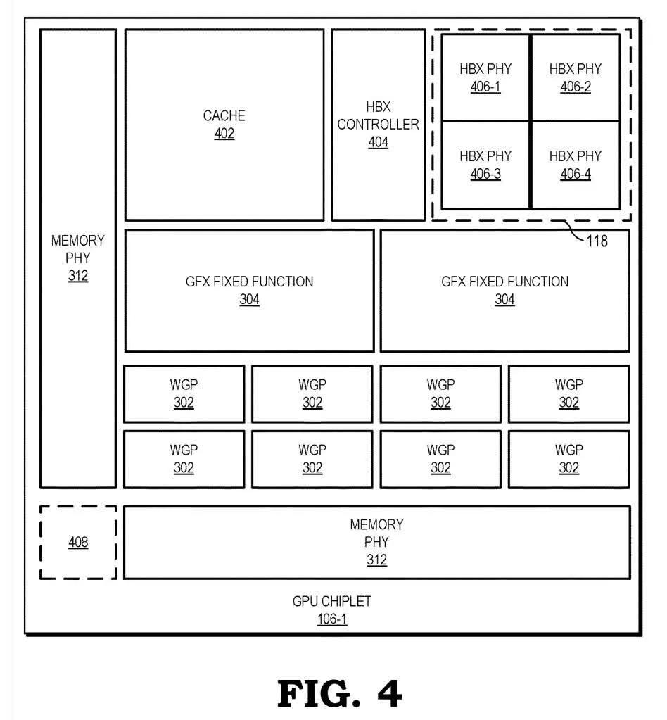
Figure 4 is a bird's eye view of one chiplet. It shows more accurately the potential locations and scales of various components. The HBX Controller (404) manages the crosslink, which the chiplet is connected to by HBX PHY (406) conductors. The small foursquare in the bottom-left corner (408) is a potential additional connectedness to the crosslink to connect more chiplets.

Source: https://www.techspot.com/news/88138-amd-patents-chiplet-gpu-design-unlike-nvidia-intel.html
Posted by: bowlingbutersest1984.blogspot.com
0 Response to "AMD patents a chiplet GPU design quite unlike Nvidia and Intel's"
Post a Comment